
SWTest Asia has SOLD OUT!
We have reached our maximum registration capacity and all deadlines have passed. We can no longer accept new registrations or substitutions. No on-site registrations will be accepted.
定員に達しましたので受付を終了させていただきました。心より感謝申し上げます。
現地会場での参加登録はお受けできませんのでご了承ください。
The 2025 program will be updated with more details in August 2025.
Last updated:
Schedule-At-A-Glance
subject to change
For details on the schedule for the 5th Annual Golf Tournament on Saturday, November 22, please visit the golf webpage.
Attendee Registration Check-In will be from 8:00 to 17:00 on both Thursday and Friday.
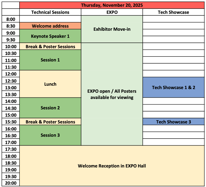
Thursday, November 20
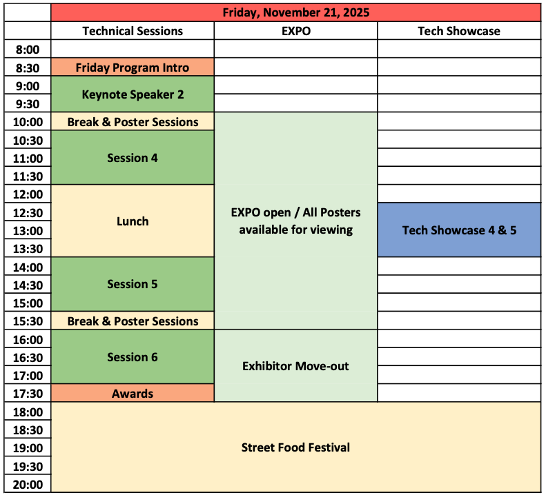
Friday, November 21
Detailed Technical Session Schedule
Wednesday, November 19
| Time | Event |
|---|---|
| 20:00 – 23:00 | EXPO Move-In/Setup |
Thursday, November 20
| Time | Event |
|---|---|
| 7:30 – 9:30 | EXPO Move-In/Setup |
| 7:30 – 17:00 | Conference Registration Check-In |
| 8:45 – 9:15 |  Welcome to SWTest Asia 2025 Welcome to SWTest Asia 2025Jerry BROZ, PhD (SWTest Conference General Chair – USA) |
| 9:15 – 10:00 |  THURSDAY VISIONARY KEYNOTE (more details) THURSDAY VISIONARY KEYNOTE (more details)Leading edge test technology and strategy for Automotive products Kazuyuki IWAGURO Vice President of HPC Business management and Operations Division (Renesas Electronics Corporation – Japan) |
| 10:00 – 10:30 | Tea Break in EXPO Hall |
| 10:00 – 10:30 | Technical Poster Session |
| 10:00 – 17:30 | SWTest Asia 2025 EXPO Open |
| 10:30 – 12:00 | Technical Session 1: Enabling HBM Test Session Chair: Eric Chia-Cheng CHANG (Intel – USA) |
| 10:30 – 11:00 |  The emergence of Advanced Memories and its impact on Probe test solutions. The emergence of Advanced Memories and its impact on Probe test solutions.Alistair LAING (Micron Technology – USA) |
| 11:00 – 11:30 |  Innovations in Testing for Truly Known Good High Bandwidth Memory Stacks Innovations in Testing for Truly Known Good High Bandwidth Memory StacksAlan LIAO (FormFactor – USA), Hiromitsu TAKASU (Advantest – Japan) |
| 11:30 – 12:00 | 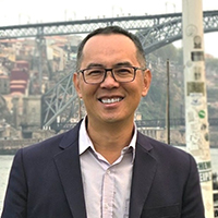 Evaluation of Probing Parameters via Post-Probe Micro Bump Pattern Analysis Evaluation of Probing Parameters via Post-Probe Micro Bump Pattern AnalysisBobby CHEN (MPI Corporation – Taiwan) |
| 12:00 – 14:00 | LUNCH in EXPO Hall |
| 12:25 – 12:45 | Tech Showcase 1 – MPI Corporation Title: Advancing High-Speed and U-Bump Test Capabilities |
| 13:25 – 13:45 | Tech Showcase 2 – Micronics Japan Co., Ltd. Title: Innovative Solutions for Semiconductor Testing |
| 14:00 – 15:30 | Technical Session 2: Probe Potpourri Session Chair: Masatomo TAKAHASHI (ACCRETECH – Japan) |
| 14:00 – 14:30 |  How AI can reduce cost and extend the lifetime of probe cards How AI can reduce cost and extend the lifetime of probe cardsNunzio RENZELLA (Advantest – Italy) |
| 14:30 – 15:00 | 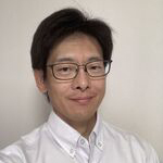 Inrush Current Suppression Technology for Probe Needle Protection Inrush Current Suppression Technology for Probe Needle ProtectionKenichi TAKANO (Keysight Technologies – Japan) |
| 15:00 – 15:30 |  Innovative Cleaning Wafer Strategies to Enhance Memory Probing Efficiency Innovative Cleaning Wafer Strategies to Enhance Memory Probing EfficiencyVictoria TRAN (Gel-Pak – USA), Keiichi RYU, Miki NOMURA, Tomonao NAKASHIMA (JEM – Japan) |
| 15:30 – 16:00 | Tea Break in EXPO Hall |
| 15:30 – 16:00 | Technical Poster Session |
| 15:35 – 15:55 | Tech Showcase 3 – FormFactor, Inc. Title: Enabling Next-Generation Devices: Trends, Challenges, and Solutions in Wafer-Level Probing for Advanced Packaging and Silicon Photonics |
| 16:00 – 17:30 | Technical Session 3: Materials Challenges Session Chair: Clark LIU (MJC – Taiwan) |
| 16:00 – 16:30 |  New probes for wafer test at highest current densities New probes for wafer test at highest current densitiesGeorg FRANZ (T.I.P.S. Messtechnik GmbH – Austria) |
| 16:30 – 17:00 |  Probe Card Analyzer Motherboard Flexibility and Performance Improvement Probe Card Analyzer Motherboard Flexibility and Performance ImprovementStefan THURMAIER (Turbodynamics GmbH – Germany) |
| 17:00 – 17:30 |  Development of a High-Hardness Pd Alloy “TK-SK” with Hardness over 600 HV for Pogo Pin Applications Development of a High-Hardness Pd Alloy “TK-SK” with Hardness over 600 HV for Pogo Pin ApplicationsKeisuke ODAKURA, Kunihiro SHIMA, Takeshi FUSE, Takeyuki SAGAE (TANAKA PRECIOUS METAL TECHNOLOGIES Co., Ltd. – Japan) |
| 17:30 – 20:00 | Kagamiwari Ceremony & Welcome Reception |
Poster Session
Session Chair: Nyi Nyi THEIN (Sandisk Corporation – Japan)
- Evaluation of Palladium Alloy Probe with Suppressed Sn Diffusion Reaction
Kenichi SATO, Tomohisa HOSHINO, Naohito ODANI (Yokowo Corporation – Japan), Shohji IKUO (Graduate School of Science and Technology, Gunma University – Japan) - Technologies to support data transmission with extremely high frequencies (400G+) on printed circuit boards
Quaid Joher FURNITUREWALA (Advantest America Inc – USA) - High Voltage DUT Power Supply IC for Automotive Grade Testing
Thomas ABIOG (Elevate Semiconductor – USA) - A Modern Low Current, Low Leakage Switch Matrix
Hai DAU, Israel ECHEVARRIA, John WILLIAMSON, Christine BUI (Spire Manufacturing, Inc. – USA) - A POGO-Type MEMS pin for Fine-Pitch Probing
Jong-Uk BU, Ho-Sub BANG, Hwangsub KOO, SangHyeop LEE, Seo KOO, Seokhwan YOO, Youngho NAM (WithMEMS – South Korea) - Applying Chiplet Concepts to Interfaces: Breaking the Barriers Holding the Industry Down
Eric SHOEMAKER, Brian BRECHT (DIS Tech – USA) - Innovative Testing Strategies for Silicon Photonic Devices in Engineering and Production Applications
Kainoa KEKAHUNA (FormFactor – USA) - Evaluation of Ultra-High-Multi Layer PCB (124L) for Probe Card
Yasuyuki SHINBO, Toshihiko OGURA (OKI Circuit Technology Co., Ltd. – Japan) - High Pin Count, High Parallelism Vertical Probe Card Characterization Strategies for HVM Automotive Bump Wafer Testing
Cameron HARKER (FormFactor – USA), Yoichi URAKAWA (FormFactor – Japan) - Reinventing Guide Plates for Vertical Probe Cards: Solving Design Constraints with Advanced Laser Drilling and Materials Science
Chris STOKES (Oxford Lasers – United Kingdom) - From Concept to Extended Validation: Localized Thermal Management for AI and GPU Wafer Testing
Klaudiusz HOLECZEK (Watttron GmbH – Germany), Klemens REITINGER (ERS electronic GmbH – Germany) - Development of low CTE LTCC material for ST substrates
Yasuo YAMAZAKI, Eiichi NAKAMURA, Shigekatsu KONO, Takahisa YAMAGUCHI (Nippon Electric Glass Co., Ltd. – Japan) - Combining Material Development & Advanced Processing into High-Quality Foils to optimize application performance and cut costs
Matthias WEGNER, Martin SENZEL, Nail AKROUTI (Heraeus Precious Metals – Germany) - Delay Characterization for FPGA PUFs Using Fully Synchronous On-Chip PLL Techniques
Kentaroh KATOH, Toru NAKURA (Fukuoka University – Japan), Haruo KOBAYASHI (Gunma University – Japan) - Automated Cause-Effect Discovery on Multivariate Time-series Data -Semiconductor production dynamics and process anomaly
ChenDing MAO, Ke LI (University of Tsukuba – Japan) - Multi-criteria Parameter Optimization for Complex Systems – Multi-Objective Scheduling Case
ChenDing MAO, Hiroto AKIZUKI, Shoyo YOSHIDA (University of Tsukuba – Japan) - J-OSAT Promotion
Akio TSUNOI, Tsuyoshi YOKOYAMA (Tera Probe – Japan)
Friday, November 21
| Time | Event |
|---|---|
| 7:30 – 17:00 | Conference Registration Check-In |
| 8:45 – 9:00 | Friday Program Overview Jerry BROZ, PhD (SWTest Conference General Chair – USA) |
| 9:00 – 10:00 |  FRIDAY VISIONARY KEYNOTE (more details) FRIDAY VISIONARY KEYNOTE (more details)Rapidus Initiatives and Logic Testing Challenges in Advanced Semiconductor Manufacturing Atsuhiko OHNO Distinguished Engineer Technology Department #5 (Wafer/Package Test), Engineering Center (Rapidus Corporation – Japan) |
| 10:00 – 10:30 | Tea Break in EXPO Hall |
| 10:00 – 10:30 | Technical Poster Session |
| 10:00 – 16:00 | EXPO Open |
| 10:30 – 12:00 | Technical Session 4: Photonics Session Chair: Alan FERGUSON (Oxford Lasers – UK) |
| 10:30 – 11:00 |  Photonic Wafer-Level Testing in the Era of AI Photonic Wafer-Level Testing in the Era of AIRoman ZVAHELSKYI, Andres MACHADO, Florian RUPP, Philipp-Immanuel DIETRICH (Keystone Photonics – Germany) |
| 11:00 – 11:30 |  Silicon Photonics Production Wafer Testing by Utilizing Advantest V93000 SOC ATE platform Silicon Photonics Production Wafer Testing by Utilizing Advantest V93000 SOC ATE platformHsu Hao CHANG, Andrew YICK, Calvin YANG, Supreet KHANAPET (Marvell – USA), Christian KARRAS, Gregor KUPKA, Tobias GNAUSCH (Jenoptik – Germany), Derek WU, Jeff JHERN, Natan CHEJANOVSKY, Shiyang DENG (Advantest – USA), Kengo SUZUKI (Advantest – Japan) |
| 11:30 – 12:00 |  A Compact OTA Measurement System with a Lens-Equipped Anechoic Chamber for Antenna-in-Package Modules A Compact OTA Measurement System with a Lens-Equipped Anechoic Chamber for Antenna-in-Package ModulesYasushi SHIRAKATA, Kenichi MITSUGI, Shoichi KOSHIKAWA, Tomohisa HOSHINO (Yokowo Co., Ltd. – Japan) |
| 12:00 – 14:00 | LUNCH in EXPO Hall |
| 12:25 – 12:45 | Tech Showcase 4 – Heraeus Precious Metals GmbH & Co. KG Title: Experience the Difference: From Material Innovation to Industry-Leading Foil Quality in Series Production |
| 13:25 – 13:45 | Tech Showcase 5 – Japan Electronic Materials Corporation Title: Generative AI and Introducing “Your Probing Partner” JEM |
| 14:00 – 15:30 | Technical Session 5: Optical Challenges Session Chair: Muru MEYYAPPAN (Lattice Semiconductors – USA) |
| 14:00 – 14:30 |  Tomonao NAKASHIMA (Japan Electronic Material Corp – Japan), Hiroki TSUTSUMI (INTER ACTION Corporation – Japan) |
| 14:30 – 15:00 | 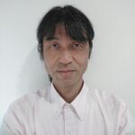 Opto-electronic probe card with single-mode fiber array for wafer-level PIC testing Opto-electronic probe card with single-mode fiber array for wafer-level PIC testingTakaharu OHYAMA, Tomohisa HOSHINO, Yasushi WATANABE, Yui NIIJIMA (YOKOWO CO., LTD. – Japan) |
| 15:00 – 15:30 |  Eclipse Dynamic Probe Card: A Novel Approach for Wafer-Level Photonic Testing with Automated Fiber Array Unit Alignment Eclipse Dynamic Probe Card: A Novel Approach for Wafer-Level Photonic Testing with Automated Fiber Array Unit AlignmentAlessia GALLI (Technoprobe – Italy), Andrew YICK, Calvin YANG, Hsu Hao CHANG (Marvell – US) |
| 15:30 – 16:00 | Tea Break in EXPO Hall |
| 16:00 – 17:30 | EXPO Move-Out |
| 16:00 – 17:30 | Technical Session 6: Advance PCB Design Session Chair: Nobuhiro KAWAMATA (FormFactor – Japan) |
| 16:00 – 16:30 | 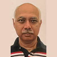 Multi-site Testing at Wafer Sort for Power Devices Multi-site Testing at Wafer Sort for Power DevicesAseem SRIVASTAVA, Tom TRAN (Teradyne, Inc – USA) |
| 16:30 – 17:00 |  Evaluating PWB Power supply characteristics of Stacked vs Single Copper Configurations Evaluating PWB Power supply characteristics of Stacked vs Single Copper ConfigurationsWai Kit K (Lincstech Co., Ltd. – Japan) |
| 17:00 – 17:30 |  Breaking Boundaries: Over 160 Layers, 10mmt Main PCB Redefining High-Density Interconnect Breaking Boundaries: Over 160 Layers, 10mmt Main PCB Redefining High-Density InterconnectSohei YASUDA (FICT Limited – Japan) |
| 17:30 – 17:35 | SWTest Asia 2025 Technical Awards |
| 17:35 – 20:00 | Japanese Street Food Festival |
Poster Session
Session Chair: Nyi Nyi THEIN (Sandisk Corporation – Japan)
- Evaluation of Palladium Alloy Probe with Suppressed Sn Diffusion Reaction
Kenichi SATO, Tomohisa HOSHINO, Naohito ODANI (Yokowo Corporation – Japan), Shohji IKUO (Graduate School of Science and Technology, Gunma University – Japan) - Technologies to support data transmission with extremely high frequencies (400G+) on printed circuit boards
Quaid Joher FURNITUREWALA (Advantest America Inc – USA) - High Voltage DUT Power Supply IC for Automotive Grade Testing
Thomas ABIOG (Elevate Semiconductor – USA) - A Modern Low Current, Low Leakage Switch Matrix
Hai DAU, Israel ECHEVARRIA, John WILLIAMSON, Christine BUI (Spire Manufacturing, Inc. – USA) - A POGO-Type MEMS pin for Fine-Pitch Probing
Jong-Uk BU, Ho-Sub BANG, Hwangsub KOO, SangHyeop LEE, Seo KOO, Seokhwan YOO, Youngho NAM (WithMEMS – South Korea) - Applying Chiplet Concepts to Interfaces: Breaking the Barriers Holding the Industry Down
Eric SHOEMAKER, Brian BRECHT (DIS Tech – USA) - Innovative Testing Strategies for Silicon Photonic Devices in Engineering and Production Applications
Kainoa KEKAHUNA (FormFactor – USA) - Evaluation of Ultra-High-Multi Layer PCB (124L) for Probe Card
Yasuyuki SHINBO, Toshihiko OGURA (OKI Circuit Technology Co., Ltd. – Japan) - High Pin Count, High Parallelism Vertical Probe Card Characterization Strategies for HVM Automotive Bump Wafer Testing
Cameron HARKER (FormFactor – USA), Yoichi URAKAWA (FormFactor – Japan) - Reinventing Guide Plates for Vertical Probe Cards: Solving Design Constraints with Advanced Laser Drilling and Materials Science
Chris STOKES (Oxford Lasers – United Kingdom) - From Concept to Extended Validation: Localized Thermal Management for AI and GPU Wafer Testing
Klaudiusz HOLECZEK (Watttron GmbH – Germany), Klemens REITINGER (ERS electronic GmbH – Germany) - Development of low CTE LTCC material for ST substrates
Yasuo YAMAZAKI, Eiichi NAKAMURA, Shigekatsu KONO, Takahisa YAMAGUCHI (Nippon Electric Glass Co., Ltd. – Japan) - Combining Material Development & Advanced Processing into High-Quality Foils to optimize application performance and cut costs
Matthias WEGNER, Martin SENZEL, Nail AKROUTI (Heraeus Precious Metals – Germany) - Delay Characterization for FPGA PUFs Using Fully Synchronous On-Chip PLL Techniques
Kentaroh KATOH, Toru NAKURA (Fukuoka University – Japan), Haruo KOBAYASHI (Gunma University – Japan) - Automated Cause-Effect Discovery on Multivariate Time-series Data -Semiconductor production dynamics and process anomaly
ChenDing MAO, Ke LI (University of Tsukuba – Japan) - Multi-criteria Parameter Optimization for Complex Systems – Multi-Objective Scheduling Case
ChenDing MAO, Hiroto AKIZUKI, Shoyo YOSHIDA (University of Tsukuba – Japan) - J-OSAT Promotion
Akio TSUNOI, Tsuyoshi YOKOYAMA (Tera Probe – Japan)